Description

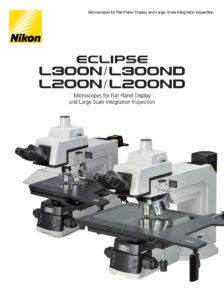
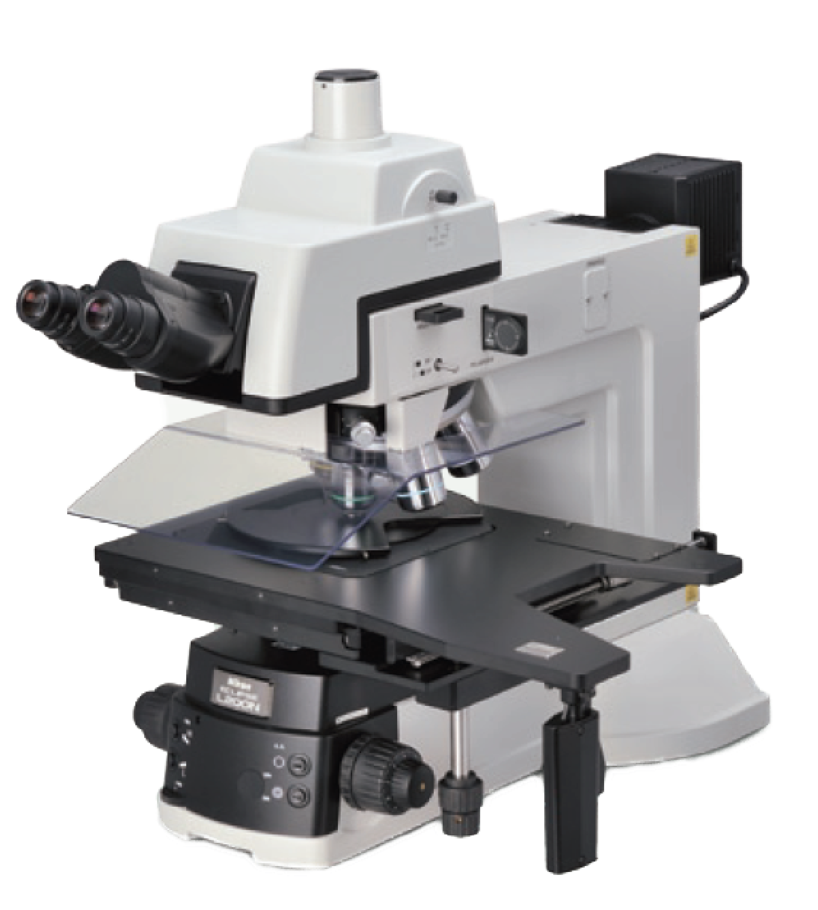
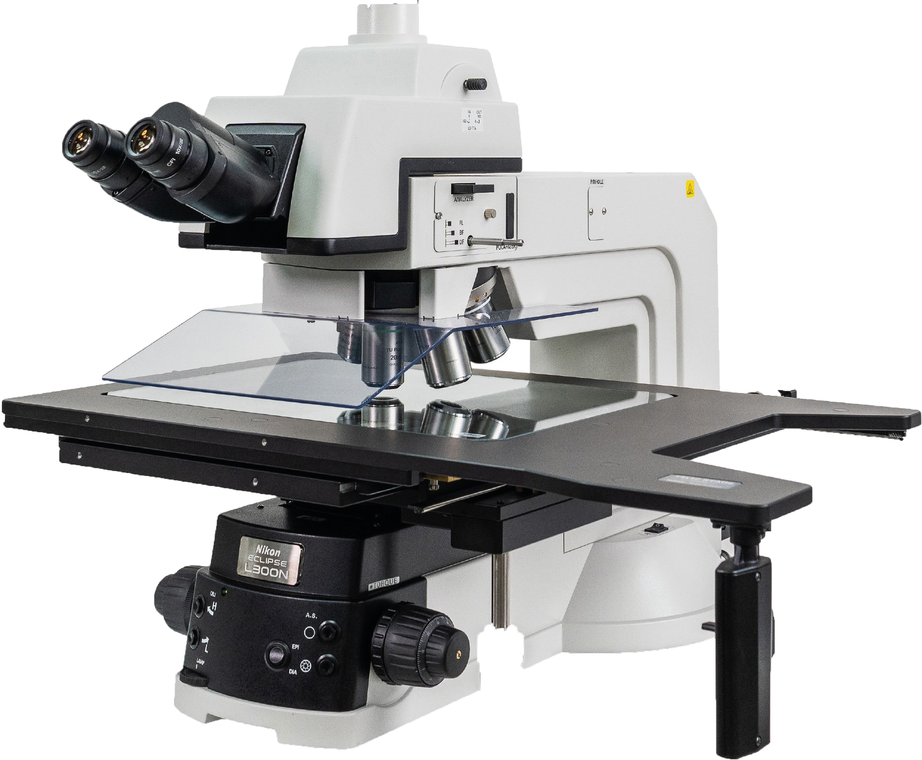
The Nikon semiconductor microscopes L200N(D) and L300N(D) are suitable for a wide range of applications, either as a pure reflected light microscope L200N/L300N, or as a combined system with reflected and transmitted light L200ND/L300ND. They have a motorized 6-position nosepiece to accommodate the Nikon high-end CFI60-2 objective series, e.g. 1x for a large overview or 100x for detailed views. The ergonomic tube can be adjusted from 0-30° for optimum adjustment to the respective user. The mechanical stage has a fixed position for XY fine adjustment and an additional coarse adjustment for comfortable handling. The systems are designed for maximum ergonomics and stability. Many settings can be made on the front of the microscope, e.g. control of the motorized nosepiece or illumination. The systems can be combined with Nikon camera and software systems and also allow control of the nosepiece, for example, via the NIS-Elements microscope software. In addition, panoramic images can be generated or depth-of-field images can be displayed. Two cross tables are available, either 8×8″ for the L200N and L200ND, or 14×12″ for the L300N and L300ND. The travel distance for the L200N and L200ND is approx. 205x205mm in reflected light and for the L200ND approx. 150x150mm in transmitted light. The travel distance for the L300N and L300ND is approx. 354x302mm in incident light and for the L300ND approx. 354x268mm in transmitted light.
(e.g. for wafer inspection, semiconductor technology)
Note: This is a general description and the illustrations are examples, you can compile the actual scope of delivery yourself.


